半导体纳米线 (NW) 激光器提供相干光源高度本地化的排放与极小小的脚印。这种激光器可能因而有革命性 photonics.1–3 的确领域的潜力,,NW 激光器预计将在未来的光电系统,即发挥关键作用,在纳米光子学中的应用集成电路片上通信和计算、 医疗保健、 超小型激光传感器和光细胞接口,用于生物 sciences.1–3 NW 激光器的极小尺寸然而,意味着它是技术上的挑战,准确操作,并将其纳入功能系统。他们从实验室环境中对现实生活的过渡,工业相关产品因此是有限的。
在过去,为新创建的操作提出了几种方法。这些包括光学镊子,4 朗缪尔-布洛杰特装配过程,5 使用显微镜探头、 6 或接触印刷 techniques.7 所有这些技术,但是,有关联的问题。例如,核武器国家必须在解决方案、 复杂设备是需要、 他们提供减少定位精度,他们不允许个别核武器国家被操纵,或异构核武器国家不能集成在同一系统内。单 NW 激光精确、 简单和高效操作因而是仍然要实现。
在研究所的光子学 (IOP) 英国斯特拉斯克莱德大学的我们因而开发一种新技术 — — 称为纳米转移印花 (纳米-TP) — — 对付的挑战单 NW 激光 manipulation.8,9 转让印刷技术 (由约翰 · 罗杰斯在 Illinois10 大学最初引入) 涉及的聚合物邮票以受控的方式捕捉半导体结构,随后将他们释放到不同基质上使用。这种方法为混合制作的各种新型光电系统提供了革命的平台 (例如,半导体激光器印上硅 substrates11 和 Led 打印上灵活和钻石 substrates12)。反过来,这些系统在许多不同的技术,可见的光通信、 灵活光电子学和光子集成电路等有很大的影响。
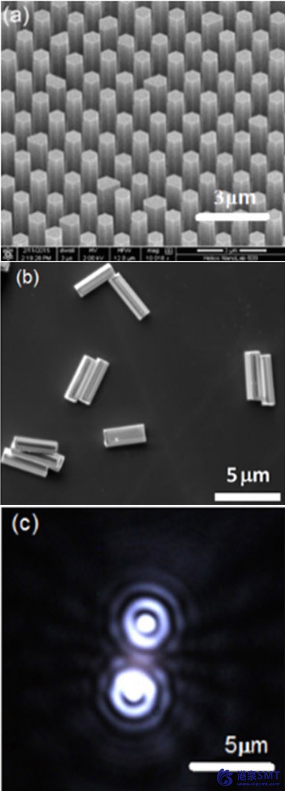
在我们使用定制的聚合物 microstamps (μ-邮票),减少了尺寸和受控的形状,来捕获/释放磷化铟 (InP) NW lasers.13 制作 (在澳洲国立大学) 我们在我们的工作中使用的激光器 nw 向我们纳米 TP 技术,我们长大垂直对齐的 InP 核武器国家在 InP 衬底上,如图 1 (a) 所示。在执行之前我们纳米 TP 研究,我们从生长基质中移除核武器国家和使用的机械手段,随机将他们分散到硅 (矽) 基片上︰ 见图 1 (b)。最后的激光器有激光的发射 — — 看到 Figure 1(c) — — ∼840 — — 890nm 波长 range.13 室温
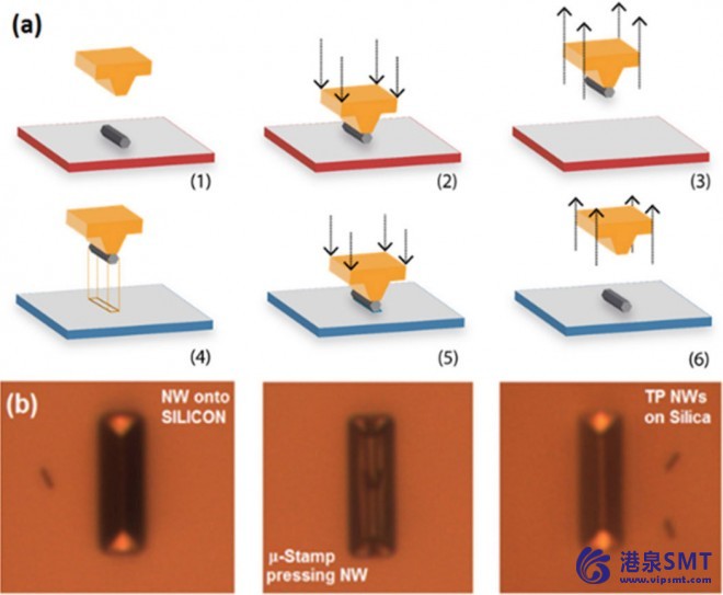
制造我们 μ 邮票,我们用聚二甲基硅氧烷 (PDMS),即,弹性和胶粘剂的聚合物,符合 NW 时紧贴着它的形状。NW 因此坚持 μ 邮票,并使其捕获。解除了我们的方法在西北部之后, 我们配合 μ 邮票 (NW 附加) 在目标位置辅助衬底上 (那里然后释放 NW)。图 2.8 中体现的不同的机制和我们纳米 TP 过程的阶段
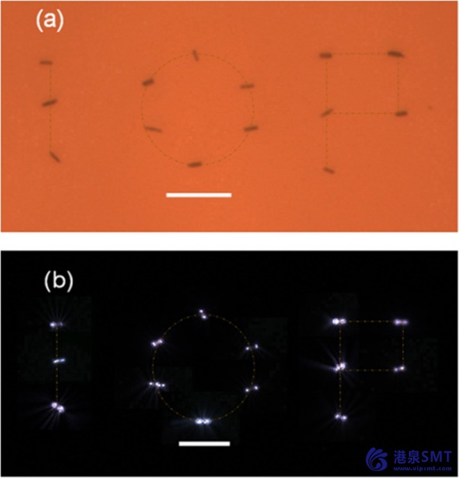
我们也习惯我们纳米 TP 方法证明精确转移的 InP 核武器国家具有不同维度 (即,435、 660,和 920nm 的直径) 从初级的硅衬底上异构的曲面 (例如,聚二甲基硅氧烷、 白炭黑或黄金) 的目标位置.8 我们找到核武器国家保留其激射的发射特性,纳米 TP 过程完成后。此外,我们的技术允许测微空间格局的形成从西北部激光器在不同衬底上。例如,我们在图 3 显示 ‘眼压’ 模式的明亮和黑暗的显微照片。我们制作这种模式 — — 在所有元素 (即,NWs) 都保留其激射的排放量 — — 用 435nm 直径 InP NWs.8
概括地说,我们开发了新型转印技术 — — 称为纳米 TP — — 使西北部激光器在异质衬底上的精确定位。我们也可以使用我们的方法将组织 NW 激光器到定制测微模式。值得注意的是,核武器国家保留其激射的排放量,甚至在 TP 协议完成后。我们的使能技术,从而开辟了 NW 激光器上功能纳米光子学系统准确地加以整合的潜力新路线。我们未来的计划涉及的纳米-TP NW 激光器纳入灯泵浦技术平台上,使用和,因而开发减少的足迹纳米光子集成电路为在信息和通信技术 (例如,集成的纳米光源在片上通信/计算系统) 和医疗服务中的应用 (例如,纳米激光器集成传感模块)。
为提供财政支助这项工作是由斯特拉斯克莱德大学 (通过斯特拉斯克莱德总理奖学金项目)、 澳大利亚研究理事会,英国工程和物理科学研究理事会 (授予 EP/I029141/1)。我们感谢澳大利亚国家的制造工厂,行为节点进入增长设施用于这项工作。
References:
1. R. Yan, D. Gargas, P. Yang, Nanowire photonics, Nat. Photon. 3, p. 569-576, 2009.
2. P. Yang, R. Yan, M. Fardy, Semiconductor nanowire: what’s next?, Nano Lett. 10, p. 1529-1536, 2010.
3. S. W. Eaton, A. Fu, A. B. Wong, C.-Z. Ning, P. Yang, Semiconductor nanowire lasers, Nat. Rev. Mater. 1, p. 16028, 2016.
4. P. J. Pauzauskie, A. Radenovic, E. Trepagnier, H. Shroff, P. Yang, J. Liphardt, Optical trapping and integration of semiconductor nanowire assemblies in water, Nat. Mater. 5, p. 97-101, 2006.
5. S. Jin, D. Whang, M. C. McAlpine, R. S. Friedman, Y. Wu, C. M. Lieber, Scalable interconnection and integration of nanowire devices without registration, Nano Lett. 4, p. 915-919, 2004.
6. H. Xu, A. Hurtado, J. B. Wright, C. Li, S. Liu, J. J. Figiel, T.-S. Luk, et al., Polarization control in GaN nanowire lasers, Opt. Express 22, p. 19198-19203, 2014.
7. Z. Fan, J. C. Ho, Z. A. Jacobson, R. Yerushalmi, R. L. Alley, H. Razavi, A. Javey, Wafer-scale assembly of highly ordered semiconductor nanowire arrays by contact printing, Nano Lett. 8, p. 20-25, 2008.
8. B. Guilhabert, A. Hurtado, D. Jevtics, Q. Gao, H. H. Tan, C. Jagadish, M. D. Dawson, Transfer printing of semiconductor nanowires with lasing emission for controllable nanophotonic device fabrication, ACS Nano 10, p. 3951-3958, 2016.
9. A. Hurtado, B. J. E. Guilhabert, M. J. Strain, N. Laurand, C. Jagadish, M. D. Dawson, Nanoscale transfer printing for heterogeneous device integration. Presented at SPIE Photonics West 2017.
10. M. A. Meitl, Z.-T. Zhu, V. Kumar, K. J. Lee, X. Feng, Y. Y. Huang, I. Adesida, R. G. Nuzzo, J. A. Rogers, Transfer printing by kinetic control of adhesion to an elastomeric stamp, Nat. Mater. 5, p. 33-38, 2006.
11. X. Sheng, C. Robert, S. Wang, G. Pakeltis, B. Corbett, J. A. Rogers, Transfer printing of fully formed thin-film microscale GaAs lasers on silicon with a thermally conductive interface material, Laser Photon. Rev. 9, p. L17-L22, 2015.
12. A. J. Trindade, B. Guilhabert, E. Y. Xie, R. Ferreira, J. J. D. McKendry, D. Zhu, N. Laurand, et al., Heterogeneous integration of gallium nitride light-emitting diodes on diamond and silica by transfer printing, Opt. Express 23, p. 9329-9338, 2015.
13. Q. Gao, D. Saxena, F. Wang, L. Fu, S. Mokkapati, Y. Guo, L. Li, et al., Selective-area epitaxy of pure wurtzite InP nanowires: high quantum efficiency and room-temperature lasing, Nano Lett. 14, p. 5206-5211, 2014.
source: http://spie.org/newsroom/6830-novel-nanoscale-transfer-printing-technique-for-precise-positioning-of-nanowire-lasers